In this column, you’ll read of flat-panel-display (FPD) circuitry patterning, which uses sputtered (see sidebar) indium tin oxide (ITO), which becomes an imperceptible maze of connecting “wires” that reside on the back side of a liquid-crystal display (LCD) screen. You’ll also learn of conductive inkjet inks and developing systems that inkjet-print antimony tin oxide (ATO) saturated inks onto polymer substrates, which accomplishes the same task as sputtering while saving the arduous masking and etching operations necessary with sputtered metals. When comparing sputtered circuitry to inkjet-printed, see sputtering as spraypainting an entire car, then blade scraping the dried paint off the windows. See the inkjet-circuit-print systems as the new guy, the one holding the masking tape and paper. Because FPDs’ (primarily LCDs and electroluminescent [EL] lamps) circuitry must inhabit the second surface of the display screen’s glass or flexible polymer, transparency requirements have made ITO, when thinly applied, the prime choice for LCD- or EL-display manufacturers. ITO can be “sputtered” onto a glass or flexible-polymer substrate in atomic-sized particles, and, after secondary treatments, the sputtered ITO becomes an imperceptible, acceptably clear maze of connecting “wires” that resides on the display screen’s back surface. Sputtering, however, may become display manufacturing’s lost technology, because developments in modern, industrial-use inkjet systems, which print a conductive ink onto a substrate, may surpass the present processes while, also, downwardly amending ITO’s present prosperity. Inkjet uses less-expensive antimony, and, better, it eliminates the troublesome masking and secondary etching process required with sputtering methods. Indium is a rare, malleable and easily fused metal — similar to aluminum or gallium — produced from the byproducts generated in zinc-ore processing. Indium also resides in iron, lead and copper ores. Interestingly, when bent, pure indium emits a high-pitched sound. Antimony is a metalloid commonly used in fire-retarding compounds, although you’ll also find it listed in alloys and semiconductors. Stibnite is antimony’s predominant source ore, but it’s also found imbedded in lead, copper and silver ores. When used in ink, antimony receives similar blending as ITO and becomes antimony tin oxide, or ATO. Note that both compounds contain tin, and, as most consumers know, tin is a soft, malleable metal used not only in Campbell’s soup cans, but in solders and various alloys. Note, too, that both alloys also contain an oxide, an oxygen-based, binary compound that helps them efficiently conduct electricity. At the moment, indium is in short supply. An August 10 Wall Street Journal (WSJ) headline — “Almost Magical Metal in Short Supply” — may have signaled inkjet-print-machine manufacturers to deploy their basic technology into the FPD industry because the ink used for inkjet printing FPD matrices contains the more easily obtained ATO. The WSJ article, written by Evan Ramstad, says that indium processors, to meet 2006 production schedules, must produce 20% more than the amount supplied today. Ore processors need approximately eight tons of raw indium to produce one ton of useable indium. Geologists say the earth’s supply of indium is 0.30 parts per million (ppm); antimony is 0.05 ppm and, comparatively, silver is 0.07 ppm. To give you an idea of price range (but not necessarily market price), Metallium Inc.’s (Norwood, MA) website, elementsales.com, lists indium at $.78/g and antimony at $.48/g. Comparatively, silver lists at $4.60/g. The amount of indium consumed strongly relates to worldwide FPD production. Canada and China lead in world production, and, not surprisingly, Japan, the major builder of FPDs, is the major indium buyer and recycler. However, as with any supply-and-demand commodity, indium-ore prices vary. Last spring, for example, the U. S. Geological Survey (USGS) office (Reston, VA) reported that flooding in China’s Hunan province had temporarily stopped indium mining, thus cutting the supply from that region. China’s mines produce a large share of the world’s indium, so sharp price increases followed the closure. Indium Corp. of America (Utica, NY), in an apparent restoration endeavor against the WSJ article, published a press release that says it’s confident of the sustained indium-metal supply. The company insists the supply imbalance occurred because of a time lag between emerging demand and the presently available supply and that “…higher prices will draw forward additional supplies which will alleviate any scarcity.” Indium has other uses. For example, Indium Corp. of America manufactures indium for FPD applications as well as alkaline batteries and solder. Indium improves battery efficiency; it’s also used in lead-free solder because, like lead, it melts at low temperature. Indium also strengthens solder. The European Union has mandated lead-free solder in electronic components. Sputtered ITO is used not only in display applications, but also on films, membrane switches, EL lamps, smart windows, transparent heaters, medical sensors and satellite blankets. Future uses include aircraft and automobile window-defrosting systems. Many popular inkjet-manufacturing companies eye the development of inkjet-technology products for new, industrial applications, especially the printing of electronic conductive inks onto display panels and other electronic applications. In FPD manufacturing, inkjet, unlike sputtering, prints a ready-to-use pattern. Carclo PLC (Wakefield, United Kingdom), a maker of high-performance, injection-molded products for the automobile, medical and communications industries, recently discovered a method to inkjet-print conductive inks while trying to print Motorola’s silver-metallic logo on customized cell phones. Because it couldn’t get the ink’s metal particles to flow through the digital printheads, Carclo contacted Xennia Technology (Hertfordshire, United Kingdom) for assistance. Carclo solved the problem and then, by continuing its research, developed a prototype machine for inkjet-printing copper-saturated inks to form radio-frequency-identification (RFID) antennas. Today, the two firms sponsor a joint-venture, start-up company titled Conductive Inkjet Technology (CIT), also in Hertfordshire. Patterning Technologies LTD (PTL), again in Hertfordshire, applies “direct-write patterning” with a proprietary (piezo) inkjet-print system that delivers conductive ink onto a prepared substrate, to produce “accurate, detailed patterns for industrial processes.” This, PTL says, replaces time-consuming and expensive photolithographic methods needed for printing circuit boards and conductor matrices for flat-panel displays. PTL applies this same technology to printing resistors, capacitors and inductors. The company has partnered with FujiFilm USA Electronic Imaging to develop manufacturing processes, equipment and consumables. PTL developed its process and materials through a SMART Feasibility Award from the U.K. Department of Trade and Industry. You’ll also find various medical and scientific uses for inkjet. The January issue of New Scientist magazine reports of a Medical University of South Carolina scientist’s inkjet system loaded with suspended cells, not ink, that recently printed 3-D tubes of living tissue onto specially prepared substrates. The article says many labs now inkjet-print arrays of DNA, proteins and cells. Magnetron Sputtering Sputtering — a metallurgical term that describes a nanotechnological coating process — moves near-invisible layers of metal (such as indium for liquid crystal display [LCD] screens) from point A to point B. In this case, point B is the glass or polymer screen substrate that contains the LCD or electroluminescent (EL) display devices. Once masked, positioned and etched, the layered indium becomes the display system’s micro-electronic circuitry. Sputtering is usually accomplished with a DC magnetron, a device that causes the transfer (and guides the movement) of electrons. Your high-school physics teacher spoke of electrons. He or she described an atom as a nucleus that comprises a specific number of positively charged protons and uncharged neutrons, all surrounded by orbits of negatively charged electrons. A DC magnetron sputter machine layers atoms (from high-grade indium) upon a substrate (a glass plate or polymer film), to create a very thin (almost invisible) metal coating. Textbooks describe a magnetron as a “crossed-field” device, because it employs both electrical and magnetic fields that act at right angles to each other. In a way, a magnetron system is similar to a cathode ray tube (CRT) in a television or computer system. A CRT encloses a negatively charged cathode that emits (shoots) a stream of magnetically guided electrons caught by an oppositely charged anode. The anode, of course, is the phosphor-coated, second side of the CRT screen. The electrons excite the phosphors to make the screen’s cells glow. A magnetron’s heated, center-positioned cathode shoots electrons toward the anode. Like the CRT, the magnetic field guides the electron’s flight path. This is the similarity between magnetron sputtering devices and television screens. After the indium sputtering, the manufacturer anneals the metallic coating. This action levels the metallic surface and, at the same time, closes the gaps between the metal particles, to increase the coating’s conductivity. At this point, the substrate appears airbrushed, as if with a transparent, silver-particled lacquer. Next, it’s etched — another finite process — to create the arrayed circuitry necessary to operate the display system. Upon completion, the electronically sprayed indium atoms, now annealed, etched and patterned, become a maze of invisible “wires” arrayed across the LCD or EL screen. Inkjet printing, as the related story explains, may eventually replace the sputtering processes. Indium, similar to aluminum or gallium, is a rare metal that’s required for building LCD and EL displays’ electronic circuitry. Shortages and new technology — industrial, piezo-inkjet printing systems using antimony-based inks — may replace indium’s present, complicated application systems, as well as the metal itself. This disclosure could reveal opportunities for inkjet systems’ manufacturers, as well as predict a reduction in LCD- and EL-display manufacturing costs.


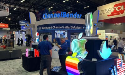
 Photo Gallery2 weeks ago
 Paula Fargo2 weeks ago
 Real Deal1 week ago
 Photo Gallery2 weeks ago
 Projects1 week ago
 Business Management1 week ago

 Dale Salamacha4 days ago